lab4:CPU(Single Cycle)
4-0 CPU核集成设计
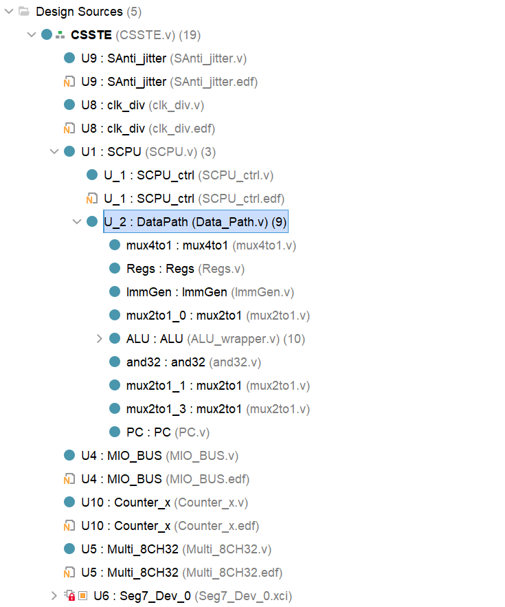
首先建构SCPU.v,并且将DataPath.v,SCPU_ctrl.v,DataPath.edf,SCPU_ctrl.edf文件导入.
SCPU.v如下:
SCPU.v
module SCPU(
    input wire MIO_ready,
    input wire [31:0] Data_in,
    input wire clk,
    input wire [31:0] inst_in,
    input wire rst,
    output wire MemRW,
    output wire CPU_MIO,
    output wire [31:0] Addr_out,
    output wire [31:0] Data_out,
    output wire [31:0] PC_out
);

    wire [1:0] ImmSel;
    wire Jump;
    wire Branch;
    wire RegWrite;
    wire [2:0] ALU_Control;
    wire ALUSrc_B;
    wire [1:0] MemtoReg;

    SCPU_ctrl U_1(
        .OPcode     (inst_in[6:2]),
        .Fun3       (inst_in[14:12]),
        .Fun7       (inst_in[30]),
        .MIO_ready  (MIO_ready),
        .ImmSel     (ImmSel),
        .ALUSrc_B   (ALUSrc_B),
        .MemtoReg   (MemtoReg),
        .Jump       (Jump),
        .Branch     (Branch),
        .RegWrite   (RegWrite),
        .MemRW      (MemRW),
        .ALU_Control(ALU_Control),
        .CPU_MIO    (CPU_MIO)
    );

    DataPath U_2(
        .clk        (clk),
        .rst        (rst),
        .inst_field (inst_in),
        .Data_in    (Data_in),
        .ALU_Control(ALU_Control),
        .ImmSel     (ImmSel),
        .MemtoReg   (MemtoReg),
        .ALUSrc_B   (ALUSrc_B),
        .Jump       (Jump),
        .Branch     (Branch),
        .RegWrite   (RegWrite),
        .PC_out     (PC_out),
        .Data_out   (Data_out),
        .ALU_out    (Addr_out)
    );

endmodule
这样测试平台就搭好了,之后我们需要完成的是:4-1将数据通路搭建完之后替换当前DataPath,4-2将控制单元搭建完之后替换当前的Control Unit,并且在4-3中进行指令扩展,4-4完成中断处理.
4-1 CPU设计之数据通路
本小节实际上是依据给出的DataPath.pdf文件写好PC.v,Data_Path.v和ImmGen.v,并组合成一个不完全版的数据通路,替换掉SCPU中的DataPath部分.
文件结构:
PC.v
module PC(
    input clk,
    input rst,
    input CE,
    input [31:0] D,
    output reg [31:0] Q
    );
    always @(posedge clk or posedge rst) begin
        if (rst) begin
            // 复位时,PC初始化为0x00000000
            Q <= 32'h00000000;
        end
        else if (CE) begin
            // 使能有效时,更新PC值
            Q <= D;
        end
    end
endmodule
在我们的DataPath中,CE使能恒置1'b1,使得PC信号可以被不断修改.
ImmSel 为 0 时,生成 I-Type 指令的立即数;为 1 时,生成 S-Type 指令的立即数;为 2 时,生成 B-Type 指令的立即数;为 3 时,生成 J-Type 指令的立即数.
ImmGen.v
module ImmGen(
    input [1:0]   ImmSel,
    input [31:0]  inst_field,
    output reg [31:0] Imm_out
);

always @(*) begin
    case(ImmSel)
        2'b00: begin
                // I-Type: imm[11:0] = inst[31:20]
                // 符号扩展到32位
                Imm_out = {{20{inst_field[31]}}, inst_field[31:20]};
            end
        2'b01: begin
                // S-Type: imm[11:5] = inst[31:25], imm[4:0] = inst[11:7]
                // 符号扩展到32位
                Imm_out = {{20{inst_field[31]}}, inst_field[31:25], inst_field[11:7]};
            end
        2'b10: begin
                // B-Type: imm[12|10:5|4:1|11] = inst[31|30:25|11:8|7]
                // imm[0] = 0 (最低位始终为0,因为分支地址是2字节对齐)
                // 符号扩展到32位
                Imm_out = {{19{inst_field[31]}}, inst_field[31], inst_field[7],
                        inst_field[30:25], inst_field[11:8], 1'b0};
            end
        2'b11: begin
                // J-Type (JAL): imm[20|10:1|11|19:12] = inst[31|30:21|20|19:12]
                // imm[0] = 0 (最低位始终为0)
                // 符号扩展到32位
                Imm_out = {{11{inst_field[31]}}, inst_field[31], inst_field[19:12],
                        inst_field[20], inst_field[30:21], 1'b0};
            end
        default: begin
                Imm_out = 32'b0;
            end
        endcase
    end
endmodule
// ImmSel 为 0 时,生成 I-Type 指令的立即数;
// 为 1 时,生成 S-Type 指令的立即数;
// 为 2 时,生成 B-Type 指令的立即数;
// 为 3 时,生成 J-Type 指令的立即数
Data_Path.v
module DataPath(
    input clk,
    input rst,
    input [31:0] inst_field,
    input ALUSrc_B,
    input [1:0] MemtoReg,
    input Jump,
    input Branch,
    input RegWrite,
    input [31:0] Data_in,
    input [2:0] ALU_Control,
    input [1:0] ImmSel,
    output [31:0] ALU_out,
    output [31:0] Data_out,
    output [31:0] PC_out
);
    wire [31:0] next_PC = PC_out + 32'd4;
    wire [31:0] Imm_out;
    wire [4:0] Rs1_addr = inst_field[19:15];
    wire [4:0] Rs2_addr = inst_field[24:20];
    wire [4:0] Wt_addr = inst_field[11:7];
    wire [31:0] Wt_data;
    wire [31:0] Rs1_data;
    wire [31:0] Rs2_data;
    wire Op2;
    wire [31:0] B;
    wire Res;
    wire [31:0] I0;
    wire [31:0] I1 = PC_out + Imm_out;
    wire [31:0] o;

    mux4to1 mux4to1(
        .s(MemtoReg),
        .I0(ALU_out),
        .I1(Data_in),
        .I2(next_PC),
        .I3(next_PC),
        .o(Wt_data)
    );

    Regs Regs(
        .clk(clk),
        .rst(rst),
        .Rs1_addr(Rs1_addr),
        .Rs2_addr(Rs2_addr),
        .Wt_addr(Wt_addr),
        .Wt_data(Wt_data),
        .RegWrite(RegWrite),
        .Rs1_data(Rs1_data),
        .Rs2_data(Rs2_data)
    );

    ImmGen ImmGen(
        .ImmSel(ImmSel),
        .inst_field(inst_field),
        .Imm_out(Imm_out)
    );

    mux2to1 mux2to1_0(
        .I0(Rs2_data),
        .I1(Imm_out),
        .sel(ALUSrc_B),
        .o(B)
    );

    ALU ALU(
        .A(Rs1_data),
        .B(B),
        .ALU_operation(ALU_Control),
        .res(ALU_out),
        .zero(Op2)
    );

    and32 and32(
        .A(Branch),
        .B(Op2),
        .res(Res)
    );

    mux2to1 mux2to1_1(
        .I0(next_PC),
        .I1(I1),
        .sel(Res),
        .o(I0)
    );

    mux2to1 mux2to1_3(
        .I0(I0),
        .I1(I1),
        .sel(Jump),
        .o(o)
    );

    PC PC(
        .clk(clk),
        .rst(rst),
        .CE(1'b1),
        .D(o),
        .Q(PC_out)
    );
    assign Data_out = Rs2_data;
endmodule
拼接之后综合并上板验证即可.
4-2 CPU设计之控制器
SCPU_ctrl.v部分的接口定义使用了瓜豪文档的定义,在此引用列举的功能:
SCPU_ctrl.v信号功能
ImmSel 用于选择生成立即数的方式,0 为 I-Type,1 为 S-Type,2 为 B-Type,3 为 J-Type.
ALUSrc_B 用于选择 ALU 的 B 输入口,0 为寄存器值,1 为立即数.
MemtoReg 用于选择写回寄存器的数据来源,0 为 ALU 输出,1 为存储器读出的值,2 为 PC+4.
Jump 用于选择 PC 的下一个值,0 为 PC+4,1 为 J-Type 指令的目标地址.
Branch 用于选择是否进行分支跳转,0 为不跳转,1 为跳转.
RegWrite 用于选择是否写回寄存器,0 为不写回,1 为写回.
MemRW 用于选择存储器的读写方式,0 为读,1 为写.
ALU_Control 用于选择 ALU 的运算方式,接口定义与 Lab2 中 ALU 的实现相同.
CPU_MIO 用于选择是否进行存储器的读写,0 为不进行,1 为进行. (实际上这个控制信号可有可无)
控制信号真值表(根据lab 4-2 21-25页得到):
| Opcode[7:2] | Funct3 | Funct7 | ALUOp | ALUControl | Branch | Jump | MemRW | ALUSrc | RegWrite | ImmSel | MemtoReg | ||
|---|---|---|---|---|---|---|---|---|---|---|---|---|---|
| R-type | add | 01100 | 000 | 0000000 | 10 | 010 | 0 | 0 | 0 | 0 | 1 | - | 00 |
| sub | 同上 | 000 | 0100000 | 同上 | 110 | 0 | 0 | 0 | 0 | 1 | - | 00 | |
| slt | 同上 | 010 | 0000000 | 同上 | 111 | 0 | 0 | 0 | 0 | 1 | - | 00 | |
| xor | 同上 | 100 | 0000000 | 同上 | 011 | 0 | 0 | 0 | 0 | 1 | - | 00 | |
| srl | 同上 | 101 | 0000000 | 同上 | 101 | 0 | 0 | 0 | 0 | 1 | - | 00 | |
| or | 同上 | 110 | 0000000 | 同上 | 001 | 0 | 0 | 0 | 0 | 1 | - | 00 | |
| and | 同上 | 111 | 0000000 | 同上 | 000 | 0 | 0 | 0 | 0 | 1 | - | 00 | |
| S-type | sw | 01000 | 010 | - | 00 | 010 | 0 | 0 | 1 | 1 | 0 | 01 | - |
| B-type | beq | 11000 | 000 | - | 01 | 110 | 1 | 0 | 0 | 0 | 0 | 10 | - |
| J-type | jal | 11011 | - | - | - | - | 0 | 1 | 0 | 1 | 1 | 11 | 10 |
| I-type | lw | 00000 | 010 | - | 00 | 010 | 0 | 0 | 0 | 1 | 1 | 00 | 01 |
| addi | 00100 | 000 | - | 11 | 010 | 0 | 0 | 0 | 1 | 1 | 00 | 00 | |
| slti | 同上 | 010 | - | 同上 | 111 | 0 | 0 | 0 | 1 | 1 | 00 | 00 | |
| xori | 同上 | 100 | - | 同上 | 011 | 0 | 0 | 0 | 1 | 1 | 00 | 00 | |
| ori | 同上 | 110 | - | 同上 | 001 | 0 | 0 | 0 | 1 | 1 | 00 | 00 | |
| andi | 同上 | 111 | - | 同上 | 000 | 0 | 0 | 0 | 1 | 1 | 00 | 00 | |
| srli | 同上 | 101 | 0000000 | 同上 | 101 | 0 | 0 | 0 | 1 | 1 | 00 | 00 |
以下是连线写出来的代码:
我本来以为到这里4-2就要收尾了,但是后面的事情复杂度又超乎了我的想象.
首先我需要根据给出的仿真平台示例进行功能仿真,先书写顶层代码进行搭建:
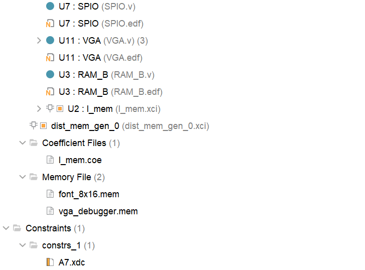
此处需要将lab0完成的ROM也导入进来,构成一个完整的SCPU测试平台.
将assembly.py运行后得出的文件program.coe输入到Vivado中